


Company
-
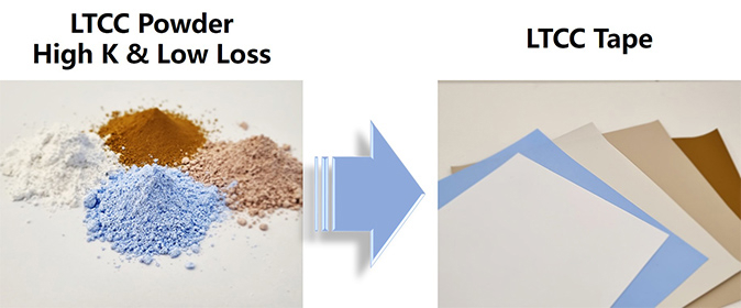
Material (Powder)
-
Powder for LTCC (RNE-40) is glass-free, featuring low dielectric losses, making it applicable to a wide range of component groups such as High-Q Capacitors, Bluetooth & W-LAN Filters, Duplexers, etc.
Tape for LTCC can be produced in a wide range of thicknesses from 30 to 250μm, based on the utilization and experience of various raw materials and additives, ready to be applied to various component groups at any time.
- 6G Candidate
Frequency Bands -
To meet the needs of materials for 5G/6G communications, it is necessary to secure materials with low dielectric and low loss characteristics, and we have internalized ceramic material stabilization and synthetic techniques in high-frequency bands, developing optimal materials through surface modification engineering.
We are developing materials that can be utilized in various industries by constructing polymers and composites that ensure improved thermal resistance and durability to enhance dielectric properties. Furthermore, we are concurrently developing materials to improve heat dissipation properties necessary for high-speed/integrated modules.
- Action item
-
- Design and synthesis of low-dielectric, low-loss ceramic compositions for mm-Wave communication bands.
- Surface activation technology for dielectric ceramic nanoparticles.
- Synthesis of organic-inorganic hybrid low-dielectric, low-loss materials.


Composite Sheet
Materials and Processes

- Low Loss:
-
- Use of electrodes
with excellent electrical
conductivity - Use of self-developed
ceramic materials with
low dielectric loss values
- Use of electrodes

- Mechanical
Reliability: -
- Similar coefficient
of thermal expansion
to semiconductor sensors - Superior mechanical
reliability compared
to PCB for sensor packaging
purposes
- Similar coefficient

- RN2 Technical Expertise:
-
- In-house technology capabilities
from raw materials to design
and processing - Selection of optimized materials
and processes depending
on the project
- In-house technology capabilities

- 3D Multilayer Circuit
Implementation: -
- Ease of Build-up Via process
- Feasible implementation
of 10 layers or more
in multilayer circuits
Road Map
- PRESENT (5G)
- NEXT-GENERATION (5G-A)
- FUTHER EVOLUTION
| 2024 | 2025 | 2026 | 2027 | 2030 | ||
|---|---|---|---|---|---|---|
| Low band | <1GHz | &Service | ||||
| Lower-Mid Band | 1~7GHz | Sample | Service | Service | ||
| Upper-Mid Band | 7~24GHz | Sample | ||||
| High Band | >24GHz | TBD | ||||
| LTCC | Composite | LTCC | Composite | Composite | ||
|---|---|---|---|---|---|---|
| Dielectric constant | - | 7.8 | <4 | 6.9 | <3.5 | <3 |
| Dielectric loss | - | <0.0015 | <0.005 | <0.001 | <0.003 | ≒0.001 |
| Tg | ℃ | >600 | >100 | >600 | >120 | >120 |
| Td | ℃ | - | >300 | - | >400 | >400 |
| CTE | ppm/℃ | 5.8 | 15~20 | 5.3 | 10~15 | 10~15 |
| Thermal conductivity | W/(m⋅K) | 3.3 | 0.5 | 4.6 | 2~3 | 2~3 |
| Moisture absorption | % | - | 0.2~0.4 | - | <0.2 | <0.2 |
| Flexural strength | Mpa | 320 | - | 230 | - | - |
| Delamination strength | kgf/cm | - | >1 | - | >1 | >1 |
| Pattern Line/space | ㎛ | 100/100 | 100/100 | 100/100 | 50/50 | 50/50 |
|---|---|---|---|---|---|---|
| Resistivity | uΩ·㎝ | <3 | <20 | <3 | <5 | <5 |
| Adhesion | - | - | 5B | 5B | 5B | 5B |
- Foundry Service
-
The Foundry Service business involves the production and supply of products using LTCC ceramic processes according to the product designs provided by customers. Our foundry services are backed by our source LTCC ceramic materials and material manufacturing technology, as well as over 20 years of LTCC process technology, providing customers with manufacturing services.
LTCC is a material with higher strength and superior heat resistance compared to plastic PCBs and is a competitive material for PCBs in extreme environments.
Additionally, we have secured supply time reduction, cost competitiveness, and quality reliability to support our customers' market entry competitiveness, based on our accumulated technical expertise and global business experience.- Strengths
-
- Complete production line from raw materials to substrates
- 100% full inspection, quality assurance
- Capabilities in material, circuit, and process design
- Accumulated technical expertise and global business experience
- Rapid response (6 weeks lead time for general POs)
Wire Boarding Pad
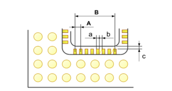
| Item | Standard | |
|---|---|---|
| a | Pad width | Min 200 um |
| b | Pad space | Min 100 um |
| c | Pad to Cavity | Min 200 um |
| A | Pad Pitch accuracy | ST ± 10% |
| B | Pad Pitch accuracy (Outer to Outer) |
ST ± 10% |
Flip Chip Pad
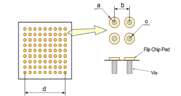
| Item | Standard | |
|---|---|---|
| a | Pad diameter | C + 100 um |
| b | Pad Pitch | a × 3 |
| c | Via diameter | Min 100 um |
| d | Distance between pad (Right end to Left end) |
ST ± 10% |
Exposed signal & Buried signal conductor
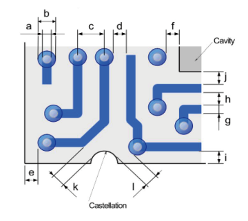
| Item | Standard | |
|---|---|---|
| a | Via diameter | Min 100 um |
| b | Via hole cover diameter | Via dia + 100 um |
| c | Via hole pitch | a × 4 |
| d | Via cover to line | Min 125 um |
| e | Via cover to substrate edge | Min 150 um |
| f | Via cover to cavity edge | Min 150 um |
| Item | Standard | |
|---|---|---|
| g | Line width | Min 100 um |
| h | Line spacing | Min 100 um |
| i | Line to substrate edge | Min 150 um |
| j | Line to cavity edge | Min 200 um |
| k | Castellation to line | Min 300 um |
| l | Castellation to line | Min 300 um |
Ground Plane
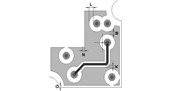
| Item | Standard | |
|---|---|---|
| K | Line to GND | Min 150 um |
| L | Isolation gap | Min 200 um |
| M | Solid plane | Min 200 um |
| N | Cavity edge to GND | Min 300 um |
| O | Substrate edge to GND | Min 300 um |
Cavity Design
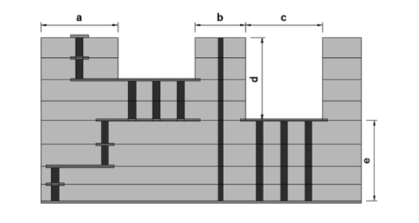
| Item | Standard | |
|---|---|---|
| a | Substrate edge to cavity edge | Min 2.0 mm |
| b | Cavity to cavity gap | Min 2.0 mm |
| c | Cavity width | Min 2.5 mm |
| d | Cavity height | Min 0.5 mm |
| e | Thickness under the cavity | Min 1.0 mm |